Introduction
The semiconductor detectors technology has dramatically changed the broad field of X- and γ-rays spectroscopy and imaging. Semiconductor detectors, originally developed for particle physics applications, are now widely used for X/γ-rays spectroscopy and imaging in a large variety of fields, among which for example, X-ray fluorescence, γ-ray monitoring and localisation, non-invasive inspection and analysis, high energy astronomy, and diagnostic medicine. The success of semiconductor detectors is due to several unique characteristics as the excellent energy resolution, the high detection efficiency and the possibility of development of compact and highly segmented detection systems. Among the semiconductors device, silicon (Si) detectors are the key detectors in the soft X-ray band (<15 keV). Si-PIN diode detectors and silicon drift detectors (SDDs) [1], operated with moderate cooling by means of small Peltier cells, show excellent spectroscopic performance and good detection efficiency below 15 keV. On the other side germanium (Ge) detectors are unsurpassed for high resolution spectroscopy in the hard X-ray energy band (>15 keV) and will continue to be the first choice for laboratory-based high performance spectrometers [2].
However, in the last decades, there has been an increasing demand for the development of room temperature detectors with compact structure having the portability and convenience of a scintillator but with a significant improvement in energy resolution and/or spatial resolution. To fulfill these requirements, numerous high-Z and wide band gap compound semiconductors have been exploited [3,4]. In fact, as demonstrated by the impressive increase in the scientific literature and technological development around the world, cadmium telluride (CdTe) and cadmium zinc telluride (CdZnTe or simply CZT) based device are today dominating the room temperature semiconductor applications scenario, being widely used for the development of X/γ-ray instrumentations [5,6].
In this paper we will focus on a particular type of detectors based on sensitive elements of CZT namely, spectrometers with spatial resolution in three dimensions. These, in fact, represent the new frontiers for applications in different fields that require increasing performance such as high energy astrophysics, the environmental radiation monitoring, medical diagnostics with PET and inspections for homeland security. The advantages offered by the possibility to reconstruct both the position of interaction of the incident photons in three dimensions (3D) and the energy deposited by each interaction are of fundamental importance for applications that require a high detection efficiency even at high energies (> 100 keV), i.e. in the Compton scattering regime, as well as a wide-field localization of the direction of incidence and a uniform spectroscopic response throughout the sensitive volume. In fact the possibility to reconstruct the photon interaction position in 3D will allow to correct from signal variations due charge trapping and material non uniformity and therefore allow to increase the sensitive volume of each detector unit without degrading the spectroscopic performance.
Principles of Operation
The typical operation of semiconductor detectors is based on collection of the charges, created by photon interactions, through the application of an external electric field. The choice of the proper semiconductor material for a radiation detector is mainly influenced by the energy range of interest. Among the various interaction mechanisms of X-rays and gamma rays with matter, three effects play an important role in radiation measurements: photoelectric absorption, Compton scattering and pair production. In photoelectric absorption the photon transfers all its energy to an atomic electron, while a photon interacting through Compton process transfers only a fraction of its energy to an outer electron, producing a hot electron and a degraded photon; in pair production a photon with energy above a threshold energy of 1.02 MeV interacts within the Coulomb field of the nucleus producing an electron and positron pair. Neglecting the escape of characteristic X-rays from the detector volume (the so called fluorescent lines), only the photoelectric effect results in the total absorption of the incident energy and thus gives useful information about the photon energy. The interaction cross sections are highly dependent on the atomic number. In photoelectric absorption it varies as Z4,5, Z for Compton scattering and Z2 for pair production.
Semiconductor detectors for X-ray and γ ray spectroscopy behaves as solid-state ionization chambers operated in pulse mode. The simplest configuration is a planar detector i.e. a slab of a semiconductor material with metal electrodes on the opposite faces of the semiconductor (Figure 1). Photon interactions produce electron-hole pairs in the semiconductor volume through the discussed interactions. The interaction is a two-step process where the electrons created in the photoelectric or Compton process lose their energy through electron-hole ionization. The most important feature of the photoelectric absorption is that the number of electron-hole pairs is proportional to the photon energy. If E is the incident photon energy, the number of electron-hole pairs N is equal to E/w, where w is the average pair creation energy. The generated charge cloud is Q0 = eE/w. The electrons and holes move toward the opposite electrodes, anode and cathode for electrons and holes, respectively (Figure 1).
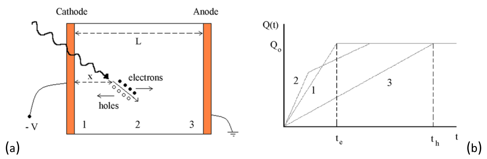
Figure 1. Planar configuration of a semiconductor detector: (a). Electron–hole pairs, generated by radiation, are swept towards the appropriate electrode by the electric field; (b) the time dependence of the induced charge for three different interaction sites in the detector (positions 1, 2 and 3). The fast rising part is due to the electron component, while the slower component is due to the holes
The movement of the electrons and holes, causes variation ΔQ of induced charge on the electrodes and it is possible to calculate the induced charge ΔQ by the Shockley–Ramo theorem [7]. The charge collection efficiency is a crucial property of a radiation detector and affects the spectroscopic performances and in particular the energy resolution. High charge collection efficiency ensures good energy resolution which also depends by the statistics of the charge generation and by the noise of the readout electronics. Therefore, the energy resolution (FWHM) of a radiation detector is mainly influenced by three contributes:

The first contribution is the Fano noise due to the statistics of the charge carrier generation. In semiconductors, the Fano factor F is much smaller than unity (0.06–0.14) [8]. The second contribute is the electronic noise which is generally measured directly using a precision pulser, while the third term takes into account the contribution of the charge collection process. Different semi-empirical relations have been proposed for the charge collection contribution evaluation of different detectors [9]. (Figure 2) shows a typical spectroscopic system based on a simple semiconductor detector. The detector signals are amplified by a charge sensitive preamplifier (CSP) and then shaped by a linear amplifier (shaping amplifier). Energy spectra are obtained by a multichannel analyzer (MCA) which samples and records the shaped signals.
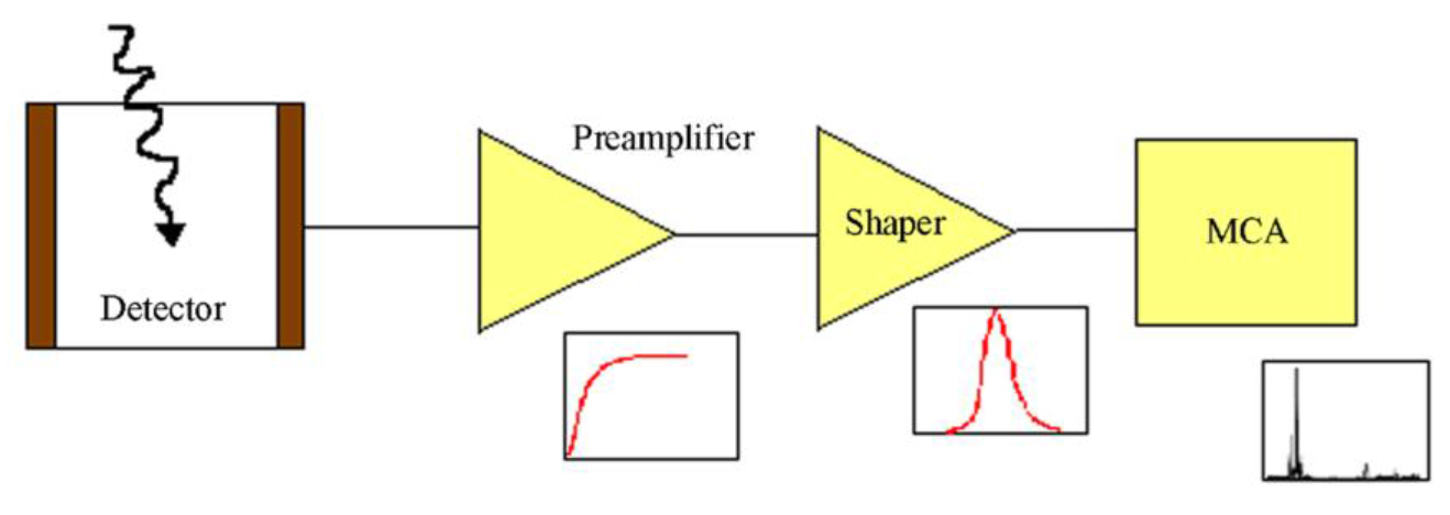
Figure 2. Block diagram of a standard spectroscopic detection system for X- and γ-rays.
3D CZT Sensor Configurations and Developments
One of the most recent development in this field regards the so called three dimensional (3D) detectors. A 3D spectrometer is, in principle, a detector divided into volume elements (voxels), each operating as an independent spectroscopic sensor. The signal produced in each voxel by the interaction of an incoming X/γ photon must be able to be is read and converted into a voltage signal proportional to the energy released. If the readout electronics of the detection system implements a coincidence logic, it will be possible to determine to some extent the history of the incident photon inside the sensitive volume by associating the energy deposits in more voxels to the same incident photon. The need for this type of sensors comes from the applications requirements. For example, in the field of hard X- and soft γ-rays astrophysics (10–1000 keV), there are promising developments of new focusing optics operating for up to several hundreds of keV, through the use of broadband Laue lenses [10] and new generation of multilayer mirrors [11]. These systems make it possible to push the sensitivity of a new generation of innovative high energy space telescopes at levels far higher (100–1000 times) than current instrumentation. To obtain the maximum return from this type of optics up to MeV, then you it is required the use of focal plane detectors with high efficiency (> 80%) even at higher energies and with that shall have also the ability to measure the energy spectrum with good spectroscopic resolution and also to localize accurately (0.1–1 mm) the point of interaction of the photons used for the correct attribution of their direction of origin in the sky.
In fact the realization of 3D spectrometers by a mosaic of single CZT crystals is not as easy as for the case of bi-dimensional imagers, mainly because to the small dimension of each sensitive unit necessary to guarantee the required spatial resolution and also for the intrinsic difficulty of packaging in 3D sensor units in which each one requires an independent spectroscopic readout electronics chain. A solution is offered by the realization of stack of 2D spectroscopic imagers [12, 13]. This configuration, is very appealing for large area detector, but has several drawbacks for application requiring fine spatial resolution in three-dimension and compactness. Indeed the distance between each 2D layer of the stack limits the accuracy and the sampling of the third spatial coordinate as well as passive materials are normally required for mechanical support.
To solve this kind of problems, in the last 10–15 years, there have been several groups that have focused their activity on the development of sensors based on high volume (1–10 cm3) crystals of CZT/CdTe capable of intrinsically operating as 3D spectrometers and therefore able to meet the requirements for certain applications, or to make more efficient and easy the realization of 3D detectors based on matrices of these basic units. The main benefits are: a limited number of required readout channels to achieve the same spatial resolution, packing optimization and a reduction of passive material between sensitive volumes. In these developments, a key role is played by the adopted electrode configurations. Various electrode configurations have been proposed and studied to improve both the spectroscopic performance and the uniformity of the response of CZT detectors compensating and correcting problems related to trapping and low mobility of the charge carriers in these materials. In fact, these electrode configurations, with the implementation of appropriate logical reading of the signals, makes it intrinsically able to determine the position of interaction of the photon in the direction of the collected charge (depth sensing) and therefore are particularly suited to the realization of 3D monolithic spectrometers without requiring a drastic increase of the electronics readout chains. In the framework of a project recently funded by the Italian Space Agency we are working on the development of a 3D CZT prototype for astrophysical applications and, in particular, on the realization of an advanced front-end electronics based on the RENA3 ASIC suitable for a flexible qualification and characterization of several CZT crystal samples. Here we report some detail about the development of this electronics.
Electronic chain for selection and qualification of 3D CZT detectors
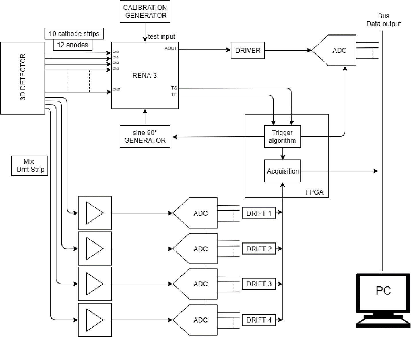
The processing of the signals provided by a 3D CZT detector required to obtain an imaging-spectroscopy device needs sophisticated electronics. The detector treated here, for example, is biased so as to provide the signals through three different types of electrodes: anodes, cathodes and drift strips. For this reason the front-end electronics has to be able to process signals of both polarities, positive and negative, in the case of cathodes and anodes, and of a polarity unknown in the case of the drift strip. The main function of the analogue front-end electronics (AFEE) is to connect the 12 anode strips and the 10 cathodes to a RENA-3 ASIC from NOVA R&D Inc. (CA, USA) used as signal readout device (RENA-3TM IC User Specifications Rev 1.31, May 11, 2015). The RENA-3 ASIC is a 36- channel charge sensitive amplifier self-triggering. Each channel includes a low-noise preamplifier, a shaper with sample/hold, and in addition a fast shaper that gives a trigger signal for coincident event detection. The signal range is selectable channel by channel over two full scales (equivalent to 200 keV and 1.3 MeV for CZT) as the peaking time that ranges from 0.1 to 40 μs. The comparator thresholds can be adjusted through an 8 bit DAC on each channel in order to obtain an accurate and uniform threshold setting. A pole-zero cancellation circuit is available for minimizing pileup errors. All these features are selectable by software and are independent for each input channel.
A very important feature for our purposes is the presence of two trigger chains, a “slow” and a “fast”, each of which has programmable thresholds, independent of each other and configurable channel by channel. Through the slow trigger chain and the associated digital register, it is possible to know which channels produced a trigger, or in other words which channels were affected by an event with energy higher than set threshold. This information allows to digitally convert only the triggered channels (sparse MODE), thus contributing to the decrease of the total acquisition time and then of the dead time. In any case, there is always the possibility to digitally convert all 36 channels, independently by the trigger condition and consequently increasing the system dead time. The slow trigger signal starts the acquisition phase sampling and holding, of the 10 cathodes and the 12 anodes signals. The acquired signals are then digitized by an external ADC, managed by an FPGA, which converts one channel at a time given the presence of a single output. Peak detector, present in each channel, allows to keep the maximum value of the signal for a necessary time to be able to convert all channels by the single external ADC. The fast trigger chain allows the time-stamp implementation within each individual channel and the generation of the system trigger. The time-stamp function is obtained through two cells that sample and hold the amplitude of two quadrature sinusoids when channel fast trigger occurs. The acquired sinusoids values are extracted and digitized using the same acquisition procedure. From the knowledge of these values it possible univocally determine to the timing informations within a period of the two sinusoids. Therefore, with this technique it is possible to establish the time interval between an event detected by two different portions of the detector belonging to two different channels of the RENA3.
Moreover, in our system the fast trigger is sent to an FPGA, in which it runs an algorithm with configurable parameters, that triggers the acquisition of the signal produced by the drift strips. The digitized data related to signal and time intervals are transferred from the FPGA to the PC, in which a software allows to calculate the energy collected by each electrode and relate it to the events recorded by the drift strips and taking into account temporal coincidences.
The block diagram of the system is shown in the figure:
Several analysis and characterization systems are being developed to study 3D-CZT detectors, that use fast ADCs and algorithms that run on FPGA, aimed at reducing the large amount of data produced by sampling. These systems have the advantage of providing to the user all the informations of each single event. On other hand the “firmware” algorithms, involved to reduce the big amount of data, are hard to optimize. Furthermore, fast components and high-performance algorithms running on FPGA, required more power than an acquisition system based on peak detector.
We are realizing a system that does not want to achieve performance of fast sampling or the processing of digital data in real-time, but wants to reach a good compromise between performance, space and power consumption requirement so that it can be well exploited in space applications.
Considerations on 3D CZT Spectrometers Applications
The development of CZT spectrometers with high 3D spatial resolution and fine spectroscopy represent a real challenge to the realization of a new class of high performance instruments able to fulfil the current e future requirements in several applications fields. The possibility to achieve also a very good detection efficiency, even at high energy (up to few MeV) [14], because of the sensitive volumes that can be obtained also by mosaic or stack of 3D sensor unit, without losing significantly their spectroscopic performance and response uniformity, together with their capability to operate at room temperature, are really appealing for application as radiation monitoring and identification [7] and homeland security as well as in industrial non-invasive controls and, in the research field, for new hard X- and soft γ-ray astronomy instrumentations. Furthermore, the fine spectroscopy (few % at 60 keV and <1% above 600 keV) and the high 3D spatial resolution (0.2–0.5 mm), that these devices can guarantee coupled with an high performance readout electronics, allow to operate not only in full energy mode, but also as Compton scattering or pair detectors if equipped with an appropriate electronics providing a suitable coincidence logic to handle multi hit events. This possibility imply that these sensors are suitable to realize wide field detector for γ-ray sources (> 100 keV) localization and detection both in ground and space applications [15]. Evaluation done using a single 3D CZT sensor, as a 4π Compton Imager, has demonstrated the possibility to obtain an angular resolution ~15° at 662 keV. This is really an excellent result in the small distance scale used to reconstruct the Compton events kinematics and can be achieved only because the good 3D and spectroscopic performance of the CZT proposed sensor units.
On the possibility to operate 3D spectrometers as Compton scattering detectors rely the appealing opportunity to utilize these devices for measurements of hard X- and soft γ-rays polarimetry. Today, this type of measurement is recognized of fundamental importance in high energy astrophysics and is one of the most demanding requirements for next space mission instrumentation in this energy range (10–1000 keV). The presence of linearly polarized photons in the incoming flux from a cosmic source determine a modulation in the azimuthal direction of Compton scattered events. A 3D spectrometer able to handle properly scattered events is intrinsically able to measure this modulation, i.e. operate as a scattering polarimeter [15]. The quality (modulation factor) of a scattering polarimeter is strictly dependent on his spatial resolution and spectroscopic performance. Several experimental measurements [16,17, 18] and simulation model have demonstrated that a detector allowing a good selection of events using both the spectroscopic and position information of each hits can achieve very high modulation factor. In particular the possibility to select events within thin layer of the sensitive volume, thanks to the intrinsic 3D segmentation of the detector (i.e. close to 90° scattering direction), drastically improve the modulation factor and therefore the reliability of the polarimetric measurements.
References
- Lechner P (2004) Novel high-resolution silicon drift detectors. X Ray Spectrometry 33; Pg No: 256.
- Eberth J, Simpson J (2006) From Ge (Li) detectors to gamma-ray tracking arrays-50 years of gamma spectroscopy with germanium detectors. Progress in Particle and Nucl Phys 60; Pg No: 283.
- Owens A, Peacock A (2004) Compound semiconductor radiation detectors. Nucl Instr and Meth in Phys Res A 531; Pg No: 18.
- Sellin PJ (2003) Recent advances in compound semiconductor radiation detectors. Nucl Instr and Meth in Phys Res A 513; Pg No: 332.
- Lebrun F (2003) ISGRI: The INTEGRAL Soft Gamma-Ray Imager. Astronomy & Astrophysics 411; Pg No: L141.
- Ogawa K, Muraishi M (2010) Feasibility Study on an Ultra-High-Resolution SPECT with CdTe Detectors. IEEE Trans. on Nucl. Sci 57; Pg No: 17.
- Wahl CG, He Z (2011) Gamma-Ray Point-Source Detection in Unknown Background Using 3D-Position-Sensitive Semiconductor Detectors. IEEE Trans On Nucl Sci 58; Pg No: 605.
- Devanathan R (2006) Signal variance in gamma-ray detectors – A review. Nucl Instr Meth in Phys Res A 565; Pg No: 637.
- Kozorezov AG (2005) Resolution degradation of semiconductor detectors due to carrier trapping. Nucl Instr Meth in Phys Res A 546; Pg No: 207.
- Frontera F (2013) Scientific prospects in soft gamma-ray astronomy enabled by the LAUE project. Proc of SPIE 8861, Pg No: 886106-1.
- Della Monica Ferreira D (2013) Hard X-ray/soft gamma-ray telescope designs for future astrophysics missions. Proc. of SPIE 886; Pg No: 886116-1.
- Watanabe S (2009) High Energy Resolution Hard X-Ray and Gamma-Ray Imagers Using CdTe Diode Devices. IEEE Trans on Nucl Sci 56; Pg No: 777.
- Judson DS (2011) Compton imaging with the PorGamRays spectrometer. Nucl Instr and Meth in Phys Res 652; Pg No: 587.
- Boucher YA (2011) Measurements of Gamma Rays above 3 MeV using 3D Position-Sensitive 20×20×15 mm3 CdZnTe Detectors. IEEE Nucl. Sci Symp Conference Rec Pg No: 4540.
- Xu D (2004) 4π Compton imaging with single 3D position sensitive CdZnTe detector. Proc of SPIE 5540; Pg No: 144.
- Curado da Silva RM (2011) Polarimetry Study With a CdZnTe Focal Plane Detector. IEEE Trans On Nucl Sci 58; Pg No: 2118.
- Antier S (2014) Hard X-ray polarimetry with Caliste, a high performance CdTe based imaging spectrometer. submitted to Experimental Astronomy.
- Lee K (2010) Development of X-ray and Gamma-ray CZT detectors for Homeland Security Applications. Proc of SPIE 7664; Pg No: 766423-1.